What are logic levels
In terms of voltage
As digital signals are binary states, two voltages are often used to represent the two states. Consider, for instance, a standard TTL circuit with a supply voltage of 5V. Suppose you are measuring the output of the circuit. One misconception is to that a “logical high” will measure 5V on while a “logical low” will measure 0V. However, this way of thinking is somewhat misleading.
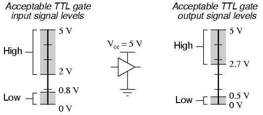
Seen above, logic levels come in ranges and the input range differs from the output range! The difference between input and output ranges, known as the noise margin, ensures the output from one TTL device can be chained to the input of another.
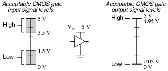
Taking a look at CMOS voltage levels, we see a greater noise margin here; the output voltage ranges are essentially Vdd and Vss. This is due to the high input impedance of CMOS devices (see here).
Side note about Vcc and Vdd: For historical reasons, Vcc often is used for bipolar (TTL) devices and means “voltage at collector.” Likewise, Vdd is used for CMOS, nMOS and pMOS devices and means “voltage at drain.”
A note on floating inputs
Now, what happens if you drive an input signal between high and low or leave it disconnected? This is known as a floating input. TTL circuits will interpret floating inputs as high (see here) however noise-induced fluctuations of just a few millivolts will cause a state switch (see here). We will return to this when discussing CMOS circuits.
In terms of source/sink
An arguably better interpretation of logic levels in terms of sources and sinks. Though equivalent to thinking about voltage levels, this offers better intuition to what is actually happening:
An output pin is logical HIGH is equivalent to saying that it is a current SOURCE.
An output pin is logical LOW is equivalent to saying that it is a current SINK.
However, to make sense of this we will have to assume that only the output can be a SOURCE and input is always a SINK. This assumption holds for most of the logic you will encounter (we will discuss I/O in more detail later).
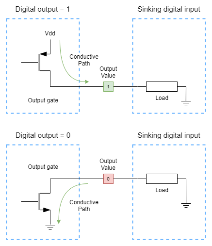
You can verify this is equivalent by Ohm’s law. Intuitively, if an output pin is HIGH, a conductive path is formed to Vdd and current flows out from the pin. Likewise, if an output pin is LOW, a conductive path is formed between ground and ground and nothing happens.
CMOS and floating inputs
While the old TTL logic is built on BJT (bipolar junction transistors), the newer and currently used CMOS is built upon MOSFETs (field-effect transistors) thus “Complementary MOS.” The “complementary” part of CMOS comes from the use of symmetrical pairs of p and n-type MOSFETs to build logic. As a result, CMOS circuits are more power-efficient than TTL and nMOS.
For our purposes, remember that nMOS will conduct when the gate voltage is high and pMOS conducts when the gate voltage is low.
Read more about nMOS and pMOS use within CMOS circuits in this lecture here.
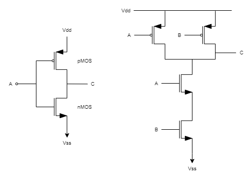
Consider the circuit on the left of a simple inverter.
- If A is HIGH, then the nMOS transistor will turn on while the pMOS will be off, allowing current to flow from C to Vss. The output will be LOW.
- If A is LOW, then the nMOS transistor will be off while the pMOS will turn on, allowing current to flow from Vdd to C. The output will be HIGH.
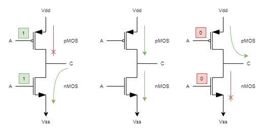
As only 1 transistor of each p-n pair turns on, this greatly reduces power consumption. However, during a state switch both MOSFETs will conduct causing a brief power spike (however the power is mainly due to capacitance, not shorting, we have yet to cover this aspect). This is also why you should never leave CMOS inputs floating.
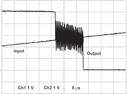
Floating CMOS inputs will cause rapid state switching at the gate (see here). Since CMOS only draws (significant) power when switching, this increases power dissipation. Therefore, the only viable way to assign “default” input states is with pull up/down resistors.
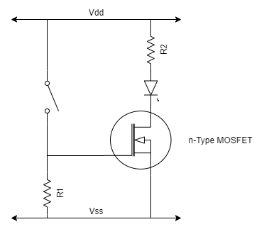
For example, here R1 is the pull-down circuit, assigning a default input value of 0 and thus the LED is off by default. If the LED is turned on, then the voltage drop across the load should be nearly Vdd (measuring from Vss) thus we see the equivalence between current sourcing and voltage levels.
Bus contention
Suppose you have many devices but only a limited amount of pins on your controller (i.e., an Arduino) - so you can only communicate with at most one device at a time. How would you wire all the devices?
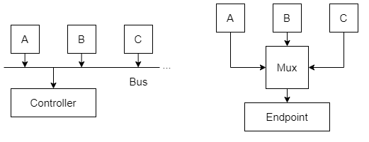
A bus is where you tie all your devices together to a common bus line as opposed to multiplexing. Many would choose to use a bus for its simplicity and extensibility. But how do you ensure only 1 device is active at a time? The first time I asked this, I thought maybe if the inactive devices outputted all 0s, then everything will be okay. Let’s see what happens when 2 devices try outputting different values at the same time:
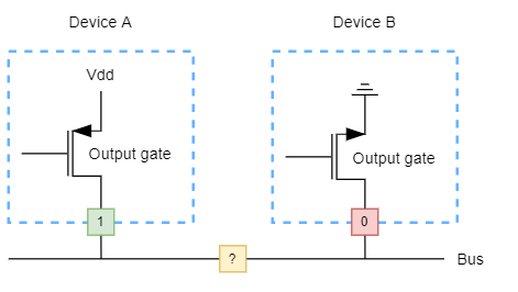
Do you see a problem? There seems to be a conductive path going from Vdd to ground!! This kind of shorting is called bus contention or just “contention.”
Note that throughout, I have neglected to draw the other transistor pair of the output gates for clarity. Just note that the other pair is always there (see below for reference).
Tristate output buffers
Obviously, we don’t want our circuits shorting out, so what’s the solution to contention? Enter, the tristate buffer. By pulling the active-low OE# signal high, we can set the buffer into a high impedance or high-Z state. The effectively removes the output from the rest of the circuit.
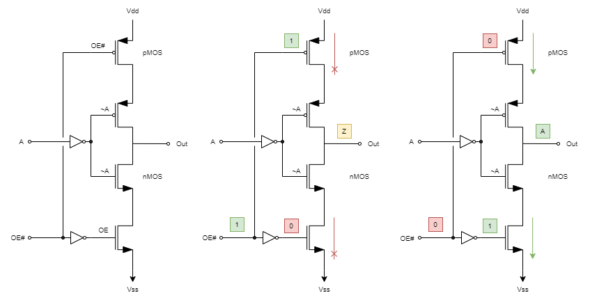
Setting OE# high disconnects the output transistor pair from Vdd and Vss. This floats the output, resolving our contention issue. However, if all devices on the bus are disabled then the bus itself will float. Remember the badness of floating CMOS inputs? Pull up/down resistors (when in doubt, go with 10kOhm) are often used to resolve this.
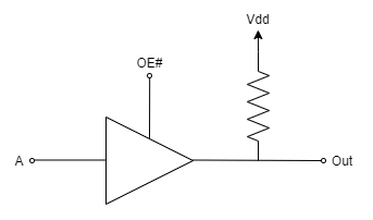
Given a high enough value (see here), little current flows through the resistor when the bus or buffer is active and will have little to no effect on the logic states. However, buses with high capacitances running at sufficient frequencies may run into issues.
As for why active low? That’s out of the scope of this post, though I think it’s mainly convention now. For further reading, see the TI Application Report Implications of Slow or Floating CMOS Inputs.
Input ESD protection
Looking through the datasheets of some devices, you might notice the maximum input voltage is equal to the supply voltage (noted Vcc below).

Note that 5V tolerant devices are a different story and have an absolute maximum VIH.
To understand why, let’s take a look at what’s going on.
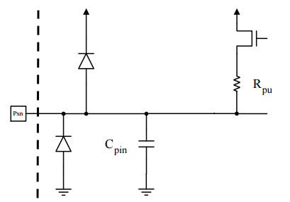
When driving a pin higher than Vcc, the sustained overvoltage causes current to flow through the upper diode into the supply rail - which can lead to local heating and damage of the diodes.
However, not all inputs employ this simple ESD diode protection.
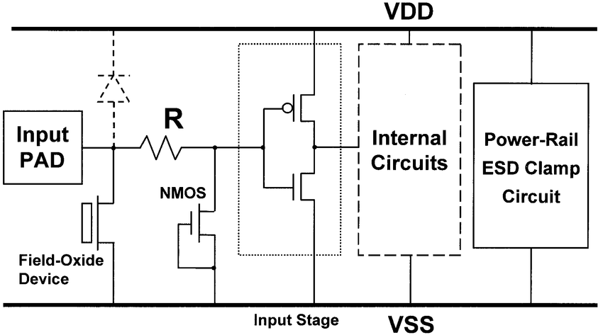
Though out of the scope of this post, you can read more about ESD (electrostatic discharge) clamps and protection circuits.